|
|
Equipe de Recherche de Prof. Dr. Hartmann Nanotechnologie et Recherche Nanostructure |
|||||||||||||||||||||||||||||||||||||
|
Adresse à contacter: |
||||||||||||||||||||||||||||||||||||||
| Institut de Physique Experimentale | ||||||||||||||||||||||||||||||||||||||
| Université de la Sarre | ||||||||||||||||||||||||||||||||||||||
| Bâtiment C6.3, 4ème Étage | ||||||||||||||||||||||||||||||||||||||
| Code Postal 151150 | ||||||||||||||||||||||||||||||||||||||
| D-66041 Sarrebruque | ||||||||||||||||||||||||||||||||||||||
| Tél.: +49681 302-3799 / 2972 | ||||||||||||||||||||||||||||||||||||||
|
Université de la Sarre |
Fax: +49681 302-3790 | |||||||||||||||||||||||||||||||||||||
|
|
|
|
|
|||||||||||||||||||||||||||||||||||
|
|
|
|
||||||||||||||||||||||||||||||||||||
| Sommaire | ||||||||||||||||||||||||||||||||||||||
| Sujets d'Examen | ||||||||||||||||||||||||||||||||||||||
| Cours | ||||||||||||||||||||||||||||||||||||||
| Travaux Pratiques Avancés | ||||||||||||||||||||||||||||||||||||||
| Séminaires | ||||||||||||||||||||||||||||||||||||||
| Formation Professionelles | ||||||||||||||||||||||||||||||||||||||
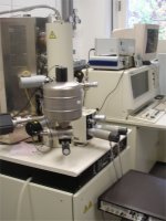
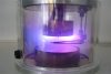
| Nanotechnologie | ||||||||||||||||||||||||||||||||||||||
| Divers Sujets | ||||||||||||||||||||||||||||||||||||||
|
28.02.2006 |
||||||||||||||||||||||||||||||||||||||