|
|
महाध्यापक डाक्टर हार्टमान के विज्ञानी समुदाय नेनो-बनावट अनुसधांन एवं नेनो-प्रद्योगिकी |
|||||||||||||||||||||||||||||||||||||
|
पता: |
||||||||||||||||||||||||||||||||||||||
| पदार्थ विज्ञान प्रयोग विभाग | ||||||||||||||||||||||||||||||||||||||
| जारलेण्ड विश्वविद्यालय | ||||||||||||||||||||||||||||||||||||||
| भवन C6.3 चौथा मजिंल | ||||||||||||||||||||||||||||||||||||||
| पत्रपेटी 151150 | ||||||||||||||||||||||||||||||||||||||
| D-66041 जारब्रूकेन | ||||||||||||||||||||||||||||||||||||||
| दूरभाष: +49681 302-3799 / 2972 | ||||||||||||||||||||||||||||||||||||||
|
जारलेण्ड विश्वविद्यालय |
फेक्स: +49681 302-3790 | |||||||||||||||||||||||||||||||||||||
|
|
|
|
|
|||||||||||||||||||||||||||||||||||
|
|
|
|
||||||||||||||||||||||||||||||||||||
| सिहांवलोकन | ||||||||||||||||||||||||||||||||||||||
| परीक्षा प्रसगं | ||||||||||||||||||||||||||||||||||||||
| पदार्थ विज्ञान वक्तृता | ||||||||||||||||||||||||||||||||||||||
| उच्च श्रेणी अभ्यास कार्य | ||||||||||||||||||||||||||||||||||||||
| सेमीनार | ||||||||||||||||||||||||||||||||||||||
| शिक्षक प्रशिक्षण | ||||||||||||||||||||||||||||||||||||||
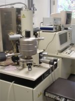
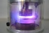
| नेनो-प्रद्योगिकी | ||||||||||||||||||||||||||||||||||||||
| विविध | ||||||||||||||||||||||||||||||||||||||
|
28.02.2006 |
||||||||||||||||||||||||||||||||||||||