|
 |
|
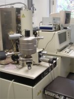
Electron-Beam Lithography is a special
technique to produce very small structures in the nm-region. A focussed
electron beam scanned the surface of the substrate, which is covered
with a electron sensitive resist material (in this experiments: PMMA).
The organic material is chemically altered by the electron beam and can
be removed after exposure. During the exposure process, the electrons
are scattered in the resist material and in the underlying substrate.
This leads to exposure in unwanted regions, a phenomena known as
proximity effect. In this experiment, the students will learn the
handling of the electron microscope, observe the effects of
backscattered electrons and will determine the characteristic constants
of the proximity effect. |